ICGOO在线商城 > IFX25401TE V50
 Datasheet下载
- 型号: IFX25401TE V50
- 制造商: Infineon
- 库位|库存: xxxx|xxxx
- 要求:
| 数量阶梯 | 香港交货 | 国内含税 |
| +xxxx | $xxxx | ¥xxxx |
查看当月历史价格
查看今年历史价格
IFX25401TE V50产品简介:
ICGOO电子元器件商城为您提供IFX25401TE V50由Infineon设计生产,在icgoo商城现货销售,并且可以通过原厂、代理商等渠道进行代购。 提供IFX25401TE V50价格参考以及InfineonIFX25401TE V50封装/规格参数等产品信息。 你可以下载IFX25401TE V50参考资料、Datasheet数据手册功能说明书, 资料中有IFX25401TE V50详细功能的应用电路图电压和使用方法及教程。
| 参数 | 数值 |
| 产品目录 | 集成电路 (IC)半导体 |
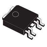
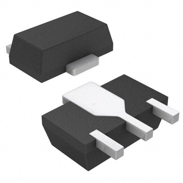
| 描述 | IC REG LDO 5V 0.4A TO252-5低压差稳压器 Low Dropout Linear Voltage Regulator |
| 产品分类 | |
| 品牌 | Infineon Technologies |
| 产品手册 | |
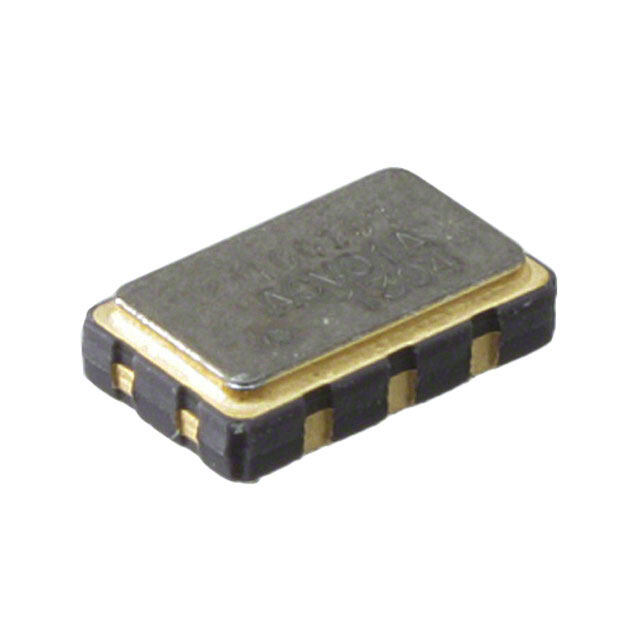
| 产品图片 |
|
| rohs | 符合RoHS无铅 / 符合限制有害物质指令(RoHS)规范要求 |
| 产品系列 | 电源管理 IC,低压差稳压器,Infineon Technologies IFX25401TE V50- |
| 数据手册 | http://www.infineon.com/dgdl/Infineon-IFX25401-DS-v01_02-en.pdf?folderId=db3a30431ff988150120802bce1d257a&fileId=db3a304320d39d590120f62a690569f7&ack=t |
| 产品型号 | IFX25401TE V50 |
| 产品种类 | 低压差稳压器 |
| 供应商器件封装 | PG-TO252-5 |
| 其它名称 | IFX25401TE V50INCT |
| 包装 | 剪切带 (CT) |
| 商标 | Infineon Technologies |
| 回动电压—最大值 | 500 mV |
| 安装类型 | 表面贴装 |
| 安装风格 | SMD/SMT |
| 封装 | Reel |
| 封装/外壳 | TO-252-5,DPak(4 引线 + 接片),TO-252AD |
| 封装/箱体 | PG-TO-252-5 |
| 工作温度 | -40°C ~ 125°C |
| 工厂包装数量 | 2500 |
| 最大工作温度 | + 125 C |
| 最大输入电压 | 40 V |
| 标准包装 | 1 |
| 电压-跌落(典型值) | 0.25V @ 250mA |
| 电压-输入 | 5.5 V ~ 40 V |
| 电压-输出 | 5V |
| 电流-输出 | 400mA |
| 电流-限制(最小值) | 400mA |
| 稳压器拓扑 | 正,固定式 |
| 稳压器数 | 1 |
| 系列 | IFX25401 |
| 负载调节 | 35 mV |
| 输出电压 | 5 V |
| 输出电流 | 400 mA |
| 输出端数量 | 2 Output |
| 输出类型 | Adjustable |
| 零件号别名 | IFX25401TEV50ATMA1 SP000623308 |

.jpg)


- 商务部:美国ITC正式对集成电路等产品启动337调查
- 曝三星4nm工艺存在良率问题 高通将骁龙8 Gen1或转产台积电
- 太阳诱电将投资9.5亿元在常州建新厂生产MLCC 预计2023年完工
- 英特尔发布欧洲新工厂建设计划 深化IDM 2.0 战略
- 台积电先进制程称霸业界 有大客户加持明年业绩稳了
- 达到5530亿美元!SIA预计今年全球半导体销售额将创下新高
- 英特尔拟将自动驾驶子公司Mobileye上市 估值或超500亿美元
- 三星加码芯片和SET,合并消费电子和移动部门,撤换高东真等 CEO
- 三星电子宣布重大人事变动 还合并消费电子和移动部门
- 海关总署:前11个月进口集成电路产品价值2.52万亿元 增长14.8%


PDF Datasheet 数据手册内容提取
IFX25401 Low Dropout Linear Voltage Regulator IFX25401TBV IFX25401TEV IFX25401TBV50 IFX25401TEV50 Data Sheet Rev. 1.02, 2012-08-24 Standard Power
Low Dropout Linear Voltage Regulator IFX25401 Features • Output Voltage Versions: 5V and Adjustable • Very Low Current Consumption • 400 mA Output Current Capability • Enable Input • Very Low Dropout Voltage • Output Current Limitation • Overtemperature Shutdown • Reverse Polarity Protection • Wide Temperature Range; -40 °C to 125 °C • Green Product (RoHS compliant) PG-TO263-5 Applications • Manufacturing and Automation • Medical Equipment • Building Management • Industrial White Goods • Security Systems IFX25401 is not qualified and manufactured according to the requirements of Infineon Technologies with regards to automotive and/or transportation applications. For automotive applications please refer to PG-TO252-5 the Infineon TLx (TLE, TLS, TLF.....) voltage regulator products. Description The IFX25401 is a monolithic integrated low dropout voltage regulator for load currents up to 400 mA. An input voltage up to 40 V is regulated to an adjustable voltage with a precision of ±2%. The device is designed for harsh environments. Therefore it is protected against overload, short circuit and overtemperature conditions by the implemented output current limitation and the overtemperature shutdown circuit. The adustable output can be configured to regulate between 2.5 V and 20 V. Due to its very low quiescent current the IFX25401 is dedicated for use in applications permanently connected to a battery. In addition the device can be switched off via the Enable input which reduces the current consumption to less than 10 μA. Type Package Marking IFX25401TBV PG-TO263-5 25401V IFX25401TEV PG-TO252-5 25401V IFX25401TBV50 PG-TO263-5 25401V50 IFX25401TEV50 PG-TO252-5 2540150 Data Sheet 2 Rev. 1.02, 2012-08-24
IFX25401 Block Diagram 1 Block Diagram Temperature Saturation Control and Sensor Protection Circuit 1 5 Ι Q Control Amplifier Buffer Bandgap Reference *) **) 2 4 3 EN VA GND *) For fixed Voltage Regulator only **) For adjustable Voltage Regulator only AEB02044 Figure 1 Block Diagram Data Sheet 3 Rev. 1.02, 2012-08-24
IFX25401 Pin Configuration 2 Pin Configuration 2.1 Pin Assignment PG-TO263-5, PG-TO252-5 GND GND 1 5 I Q 1 2 3 4 5 EN n.c. VA I GND Q AEP02560 EN n.c. VA PinConfig_PG-TO-263-5-1.vsd Figure 2 Pin Configuration (top view) 2.2 Pin Definitions and Functions PG-TO263-5, PG-TO252-5 Pin No. Symbol Function 1 I Input block to ground directly at the IC with a ceramic capacitor 2 EN Enable high level input signal enables the IC; low level input signal disables the IC; integrated pull-down resistor 3 GND Ground internally connected to heat slug 4 N.C. Not Connected for IFX25401TBV50, IFX25401TEV50 can be open or connected to GND VA Voltage Adjust for IFX25401TBV, IFX25401TEV connect external voltage divider to configure the output voltage 5 Q Output Connect a capacitor between Q and GND close to the IC pins and respect the values specified for apacitance and ESR in “Functional Range” on Page 6 Heat Slug – Heat Slug internally connected to GND; connect to PCB/System GND and heatsink area Data Sheet 4 Rev. 1.02, 2012-08-24
IFX25401 General Product Characteristics 3 General Product Characteristics 3.1 Absolute Maximum Ratings Absolute Maximum Ratings1) T = -40 °C to 150 °C; all voltages with respect to ground, (unless otherwise specified) j Pos. Parameter Symbol Limit Values Unit Test Condition Min. Max. Input I 3.1.1 Voltage V -42 45 V – I Enable EN 3.1.2 Voltage V -42 45 V – EN Voltage Adjust Input VA 3.1.3 Voltage V -0.3 10 V – VA Output Q 3.1.4 Voltage V -1 40 V – Q Temperature 3.1.5 Junction temperature T -40 150 °C – j 3.1.6 Storage temperature T -50 150 °C – stg ESD Susceptibility 3.1.7 ESD Absorption V -2 2 kV Human Body Model ESD,HBM (HBM)2) 3.1.8 V -500 500 V Charge Device ESD,CDM Model (CDM)3) 3.1.9 -750 750 V Charge Device Model (CDM) at corner pins3) 1) not subject to production test, specified by design 2) ESD susceptibility Human Body Model “HBM” according to JESD22-A114 3) ESD susceptibility Charged Device Model “CDM” according to ESDA STM5.3.1 Note:Stresses above the ones listed here may cause permanent damage to the device. Exposure to absolute maximum rating conditions for extended periods may affect device reliability. Note:Integrated protection functions are designed to prevent IC destruction under fault conditions described in the data sheet. Fault conditions are considered as “outside” normal operating range. Protection functions are not designed for continuous repetitive operation. Data Sheet 5 Rev. 1.02, 2012-08-24
IFX25401 General Product Characteristics 3.2 Functional Range Pos. Parameter Symbol Limit Values Unit Remarks Min. Max. 3.2.10 Input voltage V V + 40 V IFX25401TBV, IFX25401TEV; I Q 0.5 IFX25401TBV50, IFX25401TEV50 V > 4 V Q 3.2.11 Input voltage V 4.5 40 V IFX25401TBV, IFX25401TEV; I V < 4 V Q 3.2.12 Output Capacitor’s C 22 – µF 1) Q 3.2.13 Requirements for Stability ESR(C ) – 3 Ω 2) Q 3.2.14 Junction temperature T -40 125 °C – j 1) the minimum output capacitance requirement is applicable for a worst case capacitance tolerance of 30% 2) relevant ESR value at f = 10 kHz Note:Within the functional or operating range, the IC operates as described in the circuit description. The electrical characteristics are specified within the conditions given in the Electrical Characteristics table. 3.3 Thermal Resistance Note:This thermal data was generated in accordance with JEDEC JESD51 standards. For more information, go to www.jedec.org. Pos. Parameter Symbol Limit Values Unit Conditions Min. Typ. Max. IFX25401TBV, IFX25401TBV50 (PG-TO263-5) 3.3.1 Junction to Case1) R – 4 – K/W measured to heat thJC slug 3.3.2 Junction to Ambient1) R – 22 – K/W 2) thJA 3.3.3 – 74 – K/W footprint only3) 3.3.4 – 42 – K/W 300 mm² heatsink area3) 3.3.5 – 34 – K/W 600 mm² heatsink area3) IFX25401TEV, IFX25401TEV50 (PG-TO252-5) 3.3.6 Junction to Case1) R – 4 – K/W measured to heat thJC slug 3.3.7 Junction to Ambient1) R – 27 – K/W 2) thJA 3.3.8 – 115 – K/W footprint only3) 3.3.9 – 52 – K/W 300 mm² heatsink area3) 3.3.10 – 40 – K/W 600 mm² heatsink area3) 1) Not subject to production test, specified by design. 2) Specified R value is according to Jedec JESD51-2,-5,-7 at natural convection on FR4 2s2p board; The Product thJA (Chip+Package) was simulated on a 76.2 x 114.3 x 1.5 mm³ board with 2 inner copper layers (2 x 70µm Cu, 2 x 35µm Cu). Where applicable a thermal via array under the exposed pad contacted the first inner copper layer. Data Sheet 6 Rev. 1.02, 2012-08-24
IFX25401 General Product Characteristics 3) Specified R value is according to Jedec JESD 51-3 at natural convection on FR4 1s0p board; The Product thJA (Chip+Package) was simulated on a 76.2 × 114.3 × 1.5 mm3 board with 1 copper layer (1 x 70µm Cu). Data Sheet 7 Rev. 1.02, 2012-08-24
IFX25401 Electrical Characteristics 4 Electrical Characteristics 4.1 Electrical Characteristics Voltage Regulator Electrical Characteristics V =13.5 V; T = -40 °C to 125 °C; all voltages with respect to ground (unless otherwise specified) I j Pos. Parameter Symbol Limit Values Unit Measuring Condition Min. Typ. Max. Output Q 4.1.1 Output Voltage Accuracy1) ΔV -2 – 2 % IFX25401TBV, Q IFX25401TEV R < 50 kΩ; 2 V + 1 V ≤ V ≤ 40V; Q I V > 4.5 V; I 5 mA ≤ I ≤ 400 mA Q 4.1.2 Output Voltage V 4.9 5.0 5.1 V IFX25401TBV50 Q IFX25401TEV50 6 V ≤ V ≤ 28 V; I 5 mA ≤ I ≤ 400 mA Q 4.1.3 Output Voltage Adjustable Range3) V 2.5 – 20 V IFX25401TBV, Q,range IFX25401TEV; Refer to Page 13 4.1.4 Dropout Voltage V – 250 500 mV I = 250 mA dr Q V > 4.5 V; I V = V – V 2) dr I Q 4.1.5 Load Regulation ΔV – 5 35 mV I = 5 mA to 400 mA Q, lo Q V = 4.5 V I 4.1.6 Line Regulation ΔV – 15 25 mV V = 12 V to 32 V Q, li l I = 5 mA Q 4.1.7 Output Current Limitation I 400 600 1100 mA 2) Q 4.1.8 Power Supply Ripple Rejection3) PSRR – 54 – dB f = 100 Hz; V = 0.5 Vpp r r 4.1.9 Temperature Output Voltage Drift3) dV – 0.5 – mV/K – --------Q--- dT Data Sheet 8 Rev. 1.02, 2012-08-24
IFX25401 Electrical Characteristics Electrical Characteristics V =13.5 V; T = -40 °C to 125 °C; all voltages with respect to ground (unless otherwise specified) I j Pos. Parameter Symbol Limit Values Unit Measuring Condition Min. Typ. Max. Current Consumption 4.1.10 Current Consumption, I – – 10 μA V = 0 V q EN Regulator Disabled T ≤ 100 °C j 4.1.11 Quiescent Current I – 100 220 μA I = 1 mA; V = 5 V q Q EN I = I – I q I Q 4.1.12 Current Consumption I – 5 10 mA I = 250 mA; V = 5 V q Q EN I = I – I q I Q 4.1.13 Current Consumption I – 15 25 mA I = 400 mA; V = 5 V q Q EN I = I – I q I Q 1) influence of resistor divider on accuracy neglected 2) Measured when the output voltage V has dropped 100 mV from the nominal value obtained at V = 13.5 V. Q I 3) not subject to production test, specified by design Data Sheet 9 Rev. 1.02, 2012-08-24
IFX25401 Electrical Characteristics 4.2 Typical Performance Characteristics Voltage Regulator Current Consumption I versus Current Consumption I versus q q Output Current I Low Output Current I Q Q 16 01_IQ_IQ.VSD 1,4 02_IQ_IQLOW.VSD 14 1,2 12 VI = 13.5 V VI = 13.5 V Tj = 25 °C 1 Tj = 25 °C 10 ] ] 0,8 A A m 8 m [ [ q q 0,6 I I 6 0,4 4 0,2 2 0 0 0 100 200 300 400 0 20 40 60 80 100 I [mA] I [mA] Q Q Output Voltage V versus Dropout Voltage V versus Q dr Junction Temperature T Output Current I J Q 0,5 03_VQ_TJ.VSD 500 04_VDR_IQ.VSD T = 150 °C 0,4 450 j I = 5 mA T = 25 °C Q j 0,3 VI = 13.5 V 400 T = -40 °C j 0,2 350 0,1 300 ] ] % V m [Q 0 [ 250 R V D Δ -0,1 V 200 -0,2 150 -0,3 100 -0,4 50 -0,5 0 -40 0 40 80 120 150 0 100 200 300 400 T [°C] I [mA] j Q Data Sheet 10 Rev. 1.02, 2012-08-24
IFX25401 Electrical Characteristics Dropout Voltage V versus Maximum Output Current I versus dr Q Junction Temperature Input Voltage V I 500 05_VDR_TJ.VSD 900 06_IQMAX_VI.VSD 450 800 400 700 T = 25 °C I = 400 mA j 350 Q 600 Tj = -40 °C ] 300 ] V A T = 150 °C j m m 500 [R 250 [x D ma 400 V 200 Q, I = 100 mA I 150 Q 300 100 200 I = 10 mA V =V - 100 mV 50 Q Q Q,nom 100 0 0 -40 0 40 80 120 160 0 10 20 30 40 Tj [°C] VI [V] Region Of Stability: Output Capacitor’s ESR ESR(C ) versus Output Current I Q Q 10 07_ESR_IQ.VSD Unstable Region ] 1 Ω [ Stable ) Q C = 22 µF Region Q C V = 13.5 V ( I R S 0,1 E 0,01 0 100 200 300 400 I [mA] Q Data Sheet 11 Rev. 1.02, 2012-08-24
IFX25401 Electrical Characteristics 4.3 Electrical Characteristics Enable Function The Enable Function allows disabling/enabling the regulator via the input pin EN. The regulator is turned on in case the pin EN is connected to a voltage higher than V . This can be e.g. the battery voltage, whereby no EN,H additional pull-up resistor is needed. The regulator can be turned off by connecting the pin EN to a voltage less than V , e.g. GND. EN,L Electrical Characteristics Enable V =13.5 V; T = -40 °C to 125 °C; all voltages with respect to ground, positive current flowing into pin I j (unless otherwise specified) Pos. Parameter Symbol Limit Values Unit Measuring Condition Min. Typ. Max. 4.3.14 High Level Input Voltage V 3.5 – – V V ≥ 4.9 V EN,H Q 4.3.15 Low Level Input Voltage V – – 0.5 V V ≤ 0.1 V EN,L Q 4.3.16 High Level Input Current I 5 10 20 µA V = 5 V EN,H EN 4.4 Typical Performance Characteristics Enable Function Enabled Input Current I versus Enabled Input Current I versus EN EN Input Voltage V , (Device OFF) Enabled Input Voltage V (Device ON) I EN 600 09_IEN_VI.VSD 80 10_IEN_VEN.VSD V = 0.5 V EN 70 500 T = 150 °C 60 j 400 50 ] ] A A n µ [EN 300 V = 0.3 V [EN 40 Tj = 150 °C I EN I T = 25 °C 30 j 200 T = -40 °C j 20 100 10 V = 0.1 V EN 0 0 0 10 20 30 40 0 10 20 30 40 VI [V] VEN [V] Data Sheet 12 Rev. 1.02, 2012-08-24
IFX25401 Application Information 5 Application Information Note:The following information is given as a hint for the implementation of the device only and shall not be regarded as a description or warranty of a certain functionality, condition or quality of the device. Output I 1 5 Q Input C C R *) I IFX25401 Q 1 EN *) e.g. KL 15 2 4 3 VA Voltage GND Adjust R *) 2 *)Optional for adjustable Voltage Regulator Figure 3 Application Diagram A typical application circuit of the IFX25401 is shown in Figure 3. It shows a generic configuration of the voltage regulator with a recommended minimum number of components. The small input capacitor is not required but recommended for high frequency noise filtering. For a normal operation the fixed output voltage regulator only requires an output capacitor for stability. The adjustable output regulator requires an additional resistor network to configure the output voltage. Depending on the application conditons, additional components such as an input buffer capacitor or a reverse polarity protection diode can be considered as well. Input Filter Capacitor A small ceramic capacitor (e.g. 100nF in Figure 3) at the device’s input helps filtering high frequency noise. To reach the best filter effect, this capacitor should be placed as close as possible to the device’s input pin. The input filter capacitor does not have an influence on the stability of the device’s regulation loop. Output Capacitor C Q The output capacitor is the only external component that is required because it is part of the regulation loop. To maintain stability of this regulation loop, the IFX25401 requires an output capacitor respecting the values given in “Functional Range” on Page 6. Adjusting the Output Voltage of Variable Output Regulators IFX25401TBV, IFX25401TEV The output voltage of the IFX25401TBV and the IFX25401TEV can be adjusted between 2.5 V and 20 V by an external resistor divider connected to the voltage adjust pin VA. The VA pin is connected to the internal error amplifier comparing the voltage at this pin with the internal reference voltage (i.e. 2.5 V). Data Sheet 13 Rev. 1.02, 2012-08-24
IFX25401 Application Information 5 Q Internal V Current Reference ref and R CQ 1 22 µF 2.5 V Typical Saturation Control 4 VA R 2 AEB02804 Figure 4 External Components at Output for Variable Voltage Regulator The output voltage can be easily calculated, neglecting the current flowing into the VA pin: R +R V = -----1-------------2-×V Q R ref 2 where R <50 kΩ to neglect the current flowing into the VA pin, 2 with: • V : internal reference voltage, typically 2.5V ref • R : resistor between regulator output Q and voltage adjust pin VA 1 • R : resistor between voltage adjust pin VA and GND 2 For a 2.5 V output voltage the output pin Q has to be directly connected to the adjust pin VA. Take into consideration, that the accuracy of the resistors R and R adds an additional error to the output voltage 1 2 tolerance. Data Sheet 14 Rev. 1.02, 2012-08-24
IFX25401 Package Outlines 6 Package Outlines 4.4 10±0.2 1.27±0.1 0...0.3 A B 8.51) 3 0.05 0. ± 1 2.4 2 1) ±0. 55 0.1 5) 25 7. (1 9. 7±0.5 2.7±0.3 4. 0...0.15 5 x 0.8±0.1 0.5±0.1 4 x 1.7 8˚ MAX. 0.25 M A B 0.1 B 1) Typical Metal surface min. X = 7.25, Y = 6.9 All metal surfaces tin plated, except area of cut. GPT09113 Figure 5 PG-TO263-5 Data Sheet 15 Rev. 1.02, 2012-08-24
IFX25401 Package Outlines 6.5+0.15 -0.05 A 1) 2.3+0.05 5.7 MAX. -0.10 (5) B 0.5+0.08 1 -0.04 0. ± 1 0.9+0.20 5 -0.01 0.5 -0.2 24) ±0.1 0...0.15 9.98± 6.22 (4. 0.8 N. MI 1 0.15 MAX. 5 0. per side 5 x 0.6±0.1 0.5+0.08 -0.04 1.14 0.1 B 4.56 0.25 M A B 1) Includes mold flashes on each side. All metal surfaces tin plated, except area of cut. Figure 6 PG-TO252-5 Green Product (RoHS compliant) To meet the world-wide customer requirements for environmentally friendly products and to be compliant with government regulations the device is available as a green product. Green products are RoHS-Compliant (i.e Pb-free finish on leads and suitable for Pb-free soldering according to IPC/JEDEC J-STD-020). For further information on packages, please visit our website: http://www.infineon.com/packages. Dimensions in mm Data Sheet 16 Rev. 1.02, 2012-08-24
IFX25401 Revision History 7 Revision History Revision Date Changes 1.02 2012-08-24 Coverpage changed, Additional information about the ENABLE pin added, Disclaimer Updated 1.01 2009-10-19 Coverpage changed Overview page: Inserted reference statement to TLE/TLF series. 1.0 2009-04-28 Initial Release Data Sheet 17 Rev. 1.02, 2012-08-24
Edition 2012-08-24 Published by Infineon Technologies AG 81726 Munich, Germany © 2012 Infineon Technologies AG All Rights Reserved. Legal Disclaimer The information given in this document shall in no event be regarded as a guarantee of conditions or characteristics. With respect to any examples or hints given herein, any typical values stated herein and/or any information regarding the application of the device, Infineon Technologies hereby disclaims any and all warranties and liabilities of any kind, including without limitation, warranties of non-infringement of intellectual property rights of any third party. Information For further information on technology, delivery terms and conditions and prices, please contact the nearest Infineon Technologies Office (www.infineon.com). Warnings Due to technical requirements, components may contain dangerous substances. For information on the types in question, please contact the nearest Infineon Technologies Office. The Infineon Technologies component described in this Data Sheet may be used in life-support devices or systems and/or automotive, aviation and aerospace applications or systems only with the express written approval of Infineon Technologies, if a failure of such components can reasonably be expected to cause the failure of that life-support automotive, aviation and aerospace device or system or to affect the safety or effectiveness of that device or system. Life support devices or systems are intended to be implanted in the human body or to support and/or maintain and sustain and/or protect human life. If they fail, it is reasonable to assume that the health of the user or other persons may be endangered.
Mouser Electronics Authorized Distributor Click to View Pricing, Inventory, Delivery & Lifecycle Information: I nfineon: IFX25401TBV IFX25401TE V50 IFX25401TEV IFX25401TEV50ATMA1 IFX25401TEVATMA1 IFX25401TBVATMA1